

OUR LABORATORY IS EQUIPPED WITH VARIOUS EQUIPMENT AND CAN MEET VARIOUS REQUIREMENTS OF CHEMICAL ANALYSIS AND METALLOGRAPHIC ANALYSIS.
FOR THE SELECTED INSTRUMENT, WE ILLUSTRATE THE FEATURES IN DETAIL, THE OPERABLE FUNCTIONALITY AND ANALYSIS, IN COLLABORATION WITH Tecnologie Superficiali Srl.
SCANNING ELECTRONIC MICROSCOPE (SEM)
What is an SEM scanning electron microscope and what is it used for?
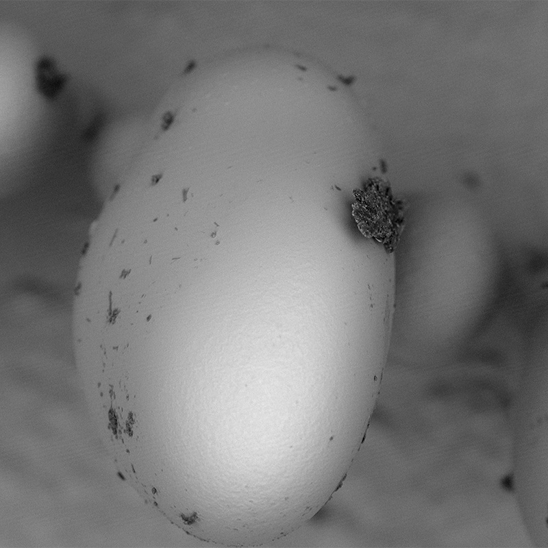
The SEM, which is the scanning electron microscope, consists of an instrument through which you can conduct a non-destructive investigation thanks to the interaction between an electron beam and the sample being examined.
It allows us to obtain information of the morphological and structural type, and thanks to the presence of an X-ray spectrometer, also important information related to the chemical nature of the analysed sample.
In a scanning electron microscope (SEM) a “probe” of very thin electrons with energy up to 15 keV is focused on the surface of the sample inside of the microscope and is induced to exert a scan in the form of a succession of parallel lines. Any phenomena are checked for the surface which has undergone the impact of the electrons.
The technology complies with ISO 9220 measurement methods.
Our laboratory is equipped with a PhenomPro X scanning electron microscope (SEM).
What is an EDS microanalysis system and what is it used for?
The chemical analysis (microanalysis) in the scanning electron microscope (SEM) is performed by measuring the energy and distribution of the intensity of X-rays generated by the electron beam on the sample using an EDS (energy dispersive spectrometry) energy scatter detector. The analysis that is produced can be either the area that is enlarged at that time, or, stopping the scan of the electron beam, of a point of interest on the sample surface (microanalysis). Since the space portion excited by the electron beam, which produces the spectrum X, is in the range of a few microns, the SEM + EDS is a powerful tool for the investigation of solids which are chemically inhomogeneous at a microscopic scale.


What can we observe and analyse at Metalcoating?
- morphological observations of samples of various interests, metallurgical, ceramic and electronic
- Qualitative analysis and processing of X-ray spectra of polished, rough and semi-gloss samples
- Quantitative microanalysis of natural and synthetic materials, polished or rough
- Defectiveness
- Contamination of the surfaces
- Elemental composition
- Nano particles
What are the characteristics that an analysis sample should have?
The maximum extent of the sample is 25 mm diameter x 30 mm deep, for higher dimensions it is necessary to cut the sample.
In our laboratory, we have available means that allow us to incorporate your samples in suitably selected resins based on the type of analysis required and lapping machines that allow us to polish your samples through the use of disks and diamond paste. Then we can proceed to the X-EDS quantitative analysis of the sample
What magnification can be achieved?
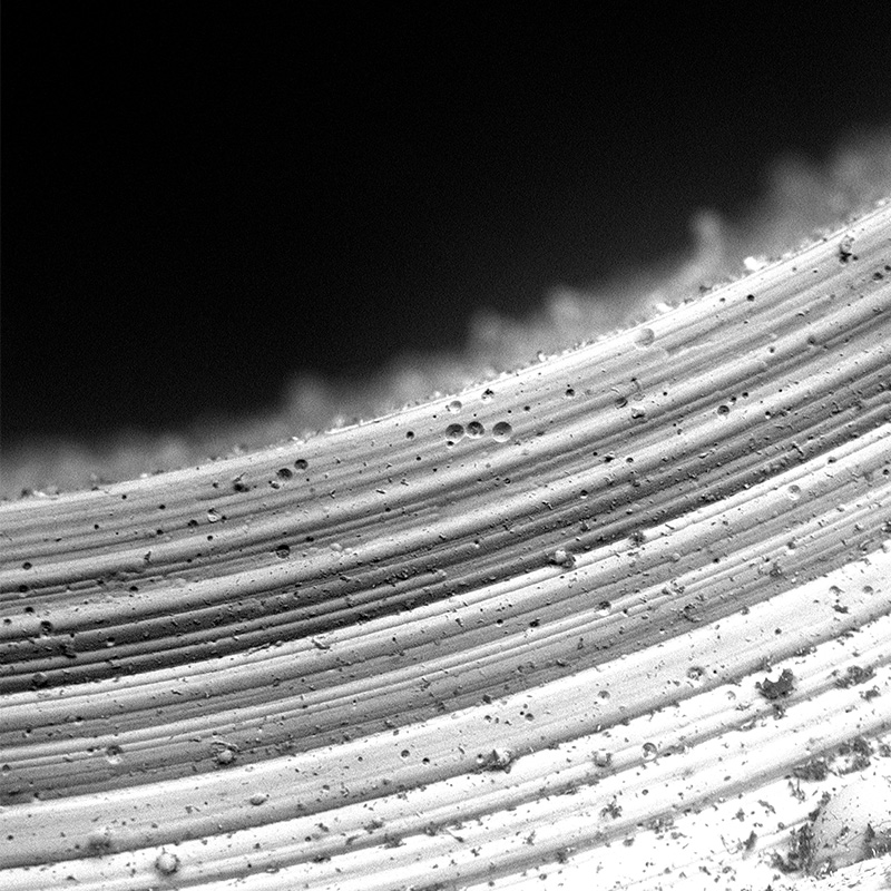
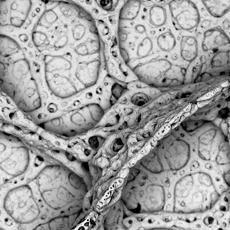
The magnification produced by a scanning electron microscope is the ratio between the size of the final image produced and the field explored by the electron beam on the sample. Normally the magnification can range from 80 to 130.000x and the resolving power can go up to 14nm (140 Angstrom). Naturally, with a much more conductive base and coating, if any, it is much easier to reach the limit of the instrument.
Which elements is it possible to identify?
All elements of the periodic table from carbon onwards
Characteristics of our microscope
- Scope of magnification 80 – 130.000x
- Resolution ≤ 14nm
- Range of detectable elements: C – At
- Source of long duration and high brightness (CeB6)
- Variable voltage range: from 4.8kV to 15kV
- Loading of the sample in less than 30 seconds
- Colour camera for navigation on the sample: zoom 20 – 120x
Qualitative and semi quantitative analysis - development of X-ray spectra of natural or raw samples - semi-finished
You can perform the SEM-EDS analysis on unprocessed, coarse or semi-polished and polished samples. You can determine the elements (major, minor and trace) having an atomic number equal to or greater than 6, with different sensitivity as a function of their atomic mass and analytical matrix.
The detectable limit values for major elements, in the X-EDS systems, are of the order of 2000 ppm (0.2%). It is possible to use fragments, platelets, portions of material, chip lengths, powders or granules, that will be mounted on suitable supports.
Quantitative analysis of polished samples
In our laboratory, we have available means that allow us to incorporate your samples in suitably selected resins based on the type of analysis required and lapping machines that allow us to polish your samples through the use of disks and diamond paste. Then we can proceed to the X-EDS quantitative analysis of the sample. The results are obtained for comparison with certified international standards. The analysed elements are, as in the previous case, all elements starting from atomic number 6. The most commonly analysed are: F, Na, Mg, Al, Si, P, S, Ca, K, Ti, Cr, Mn, Fe, Co, Ni, Cu, Zn, Ba. On particular samples, it is possible to analyse virtually all elements, with particular regard to standardisation for the following: Sc, Ga, Ge, As, Se, Rb, Sr, Y, Zr, Nb, Mo, Ru, Rh, Pd, Ag, Cd, Sn, Sb, Te, La, Ce, Pr, Nd, Sm, Gd, Dy, Er, Yb, Hf, Ta, W, Os, Ir, Pt, Au, Tl, Pb, Bi, Th, U.
Principle of operation
The configuration and arrangement of the detectors of the emitted electrons is such that they are able to take advantage of the peculiarities of the emission mechanism. In particular, the secondary electrons are used for the construction of images magnified up to 130,000x and resolved up to 14nm thanks to the fact that due to the low energy which comes from the most superficial layers of the sample, while the primary electrons are used for the identification of the presence of different compounds in a heterogeneous sample, as the intensity with which they emerge is a direct function of the average atomic number of the substance hit with the primary ray.
The emitted electron current is collected by the detectors and amplified simultaneously with the scanning of the electron beam on the sample, the variations in the strength of the resultant signal are used to vary the brilliance of the trace of the electron beam which makes a scan on a synchronic fluorescent screen with the electron beam on the sample.

